
Cryogenic Computing Laboratory / Kyushu University
Research
Our research connects superconducting devices and circuits, computing systems, and the tools that take an integrated circuit from design to test.
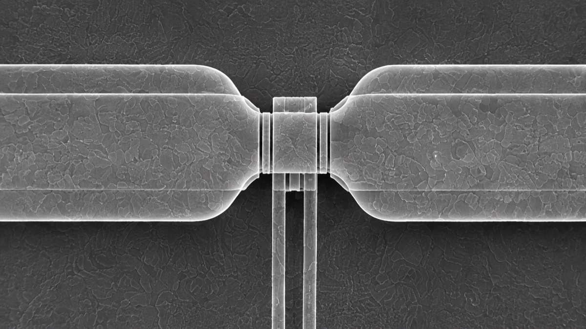
Superconducting devices & circuits
We study superconducting devices and circuits based on AQFP, SFQ, and related technologies, covering both conventional digital circuits and neuron circuits.
AQFP & SFQ
Device and circuit approaches that form the building blocks of superconducting integrated circuits.
Digital circuits
Logic and functional circuits for digital information processing, with attention to circuit behavior and implementation.
Neuron circuits
Superconducting circuit implementations of neuron functions and their connections to neural-network hardware.
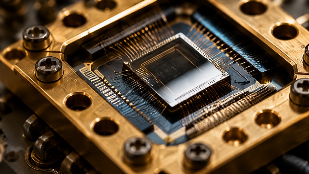
Computing systems & quantum control
At the system level, we connect superconducting circuit capabilities with the requirements of machine learning, neural networks, and quantum control.
Machine-learning accelerators
Accelerator architectures that map machine-learning computation onto superconducting hardware.
Neural networks
Hardware implementations of neural networks, linking neuron-level circuits with network-level computation.
Quantum-control circuits
Circuits and system architectures for quantum control, including their interfaces within cryogenic systems.
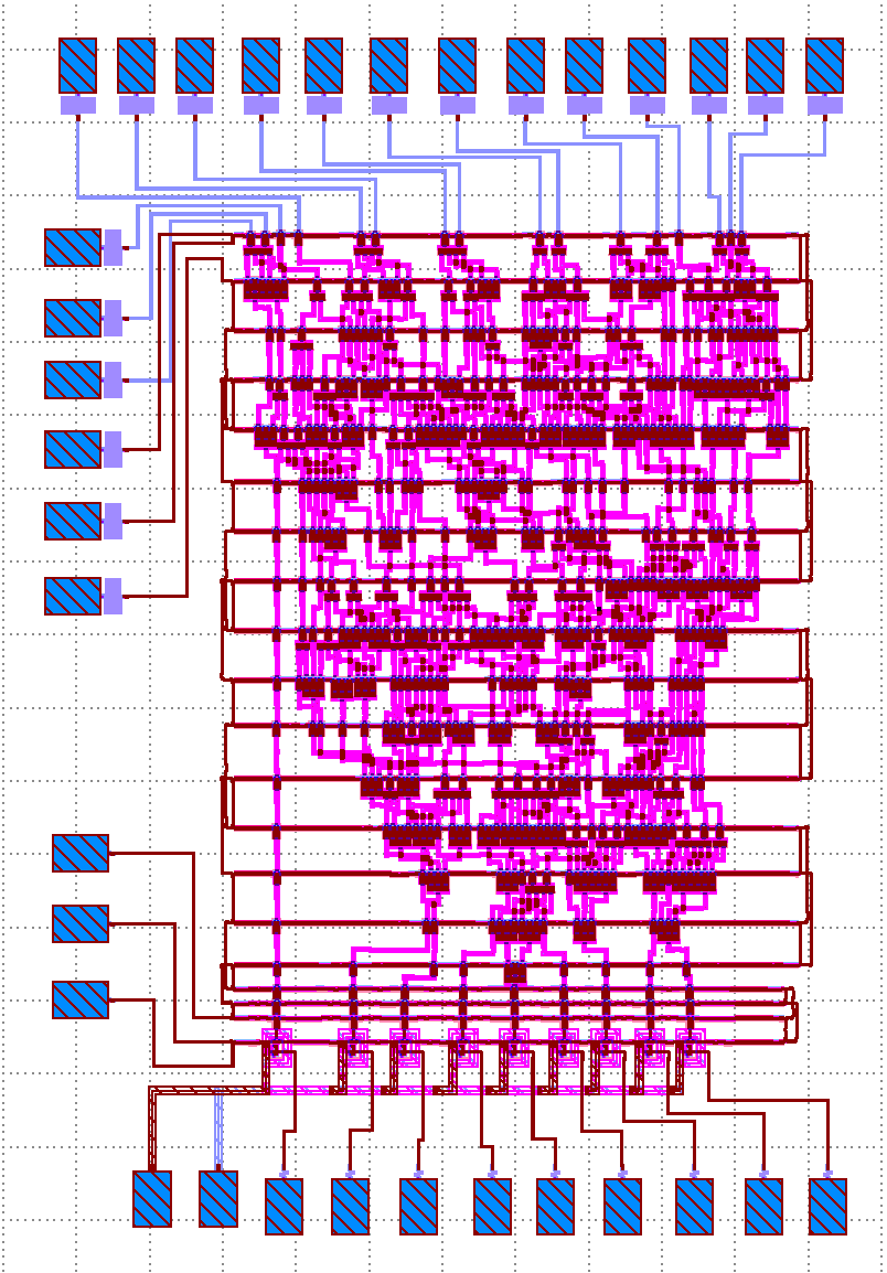
C2Lab · ICSM 2026 · 8-bit KSA
Full-stack superconducting IC design
We develop EDA tools and design methods for superconducting integrated circuits across the full stack, connecting design and implementation with measurement and test.
Design & verification
Workflows connecting circuit design, simulation, verification, and physical implementation.
From design to test
A connected workflow from design intent and circuit layout to test, with measurement results informing the next design iteration.
Large language models
Integrating LLM assistance into the design workflow, exploring support for design development, verification, and interpreting test results.
- Design
- Simulation
- Verification
- Layout
- Measurement & test
- Feedback
Explore the research record or discuss a research direction with us.
Browse publications Research with us